
With the development of science and technology, semiconductor chips are being widely used in various fields. High quality chip carriers are crucial to ensure the performance of chips during semiconductor chip manufacturing. This article will briefly introduce the manufacturing process of semiconductor chip carriers from materials to finished products.
Semiconductor chip carriers are mainly made of three materials: ceramics, metals and plastics.
Ceramic Materials: Ceramic materials have high thermal conductivity and good chemical stability. They are currently the most widely used semiconductor chip carrier materials. Commonly used ceramic materials include alumina, silicon nitride, aluminum nitride, etc.

Metal Materials: Copper alloys are commonly used metal materials for making semiconductor chip carriers. Copper alloys have high thermal conductivity, which helps chip heat dissipation, and are widely used for high-power chip carriers.

Plastic Materials: Plastic materials have low cost and are used for some low-end chips that do not have high requirements on thermal conductivity. Commonly used plastic materials include polyimide, Teflon, etc.

Aluminum Alloys: Have excellent thermal conductivity and are commonly used for heat dissipation chip carriers.

Epoxy Glass Fabric: Have excellent electrical insulation properties and are used for carriers for electrical performance testing.

Seamless Steel: High hardness and corrosion resistance, used for cutting and polishing carriers.

The parameters such as thermal expansion coefficient, mechanical strength and electrical conductivity of the materials must match the semiconductor materials to prevent adverse effects of stress and potential.
The design of the carrier must meet the size requirements of the chip, and provide precise positioning and firm fixing. Common designs include slot type, suction and mechanical clamping:
Slot type carriers use slots matched with the back surface of the chip to achieve accurate positioning.
Suction carriers use vacuum suction to adsorb the chip surface. Easy to operate but with slightly lower positioning accuracy.
Mechanical clamping uses bolts and other mechanical means to clamp the chip. Reliable but need to avoid damaging the chip.
Ceramic substrate manufacturing: Ceramic powder is made into a solid block, then cut and polished to obtain the ceramic substrate. Alumina ceramic is generally prepared by sintering; silicon nitride ceramic is prepared by hot pressing and sintering.
Plastic substrate molding: Thermoplastic plastic particles are heated and melted, injected into a mold and cooled to obtain the plastic substrate.
Metal substrate machining: Numerical control machine tools are used to cut, polish and mechanically process the metal plates to obtain smooth and flat metal substrates.
Photolithography: Using photoresist and mask templates, interconnect circuit patterns are fabricated on the substrate.
Solder coating: Solder paste is coated on the circuit pattern of the substrate, with lead or lead-free alloy as the main component.
Surface treatment: Electropolishing, electrophoresis surface treatment, coating, etc. to improve surface quality.
Packaging finished products: The fabricated carriers are cleaned, dried, and then packed in boxes to obtain the final products.
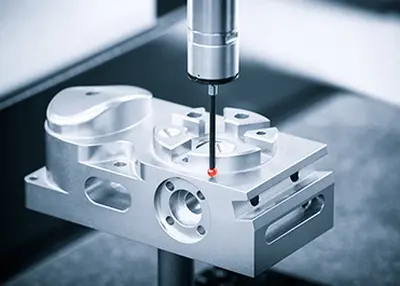
To ensure the reliability of chip carriers, strict quality control must be carried out on aspects such as materials, dimensions, and surface roughness during manufacturing. Commonly used detection methods include visual inspection, noise testing, shear testing, etc.
Optical inspection: Check key structural dimensions and positional tolerances.
Material testing: Check composition, mechanical properties and other parameters.
Electrical performance testing: Test the electrical insulation of the carrier on a simulated chip.
Cleaning and drying: Remove surface contaminants to ensure cleanliness.
Anti-static packaging: Use conductive materials to avoid static interference.
Only through strict quality management can chip carriers with stable and excellent performance be produced.
Ceramic and metal materials have significantly better thermal conductivity than plastic materials. Therefore, ceramics and metals are preferred for applications with high heat dissipation requirements. Among them, silicon nitride ceramic has the highest thermal conductivity and is an ideal heat dissipation material.
The biggest advantages of plastic carriers are low cost and high production volume; they are also easy to process and lightweight. However, plastics have poor thermal conductivity and high temperature performance, making them unsuitable for high-power chips.
When the chip power is high and the heat dissipation requirement is extremely demanding, a metal substrate with good thermal conductivity is needed to improve heat dissipation.
Sintering. The sintering process determines the densification and mechanical strength of the ceramic substrate. Controlling the sintering process parameters is crucial for obtaining high quality ceramic substrates.
Surface roughness directly affects the contact performance between the chip and the carrier. Therefore, scanning tunneling microscopy is the best method for detecting surface roughness and evaluating surface quality of substrates.
Photolithography uses ultraviolet light through a mask template to expose circuit patterns onto a photosensitive material. After development, the printed circuit board pattern is obtained. This is a key process for fabricating interconnect circuits for chip carriers.
The above briefly introduces the full process of semiconductor chip carrier manufacturing from materials to production. It is believed this can enhance the understanding of the chip carrier manufacturing process. If you have any other questions about the article, please feel free to discuss.
 Basic Parts of CNC Lathe and Their MaintenanceOctober 20, 2023CNC lathes and steering centers are highly accurate and efficient automatic machine tools. The machine is equipped with a multi-station turret or power turret for a wide range of machining capabilities. It can handle linear cylinders, tilting cylinders, arcs and a variety of complex workpieces such as threads, grooves, worms, etc.view
 The Difference Between Precision Sheet Metal Fabrication and Ordinary Sheet Metal FabricationSeptember 27, 2023In recent years, as the market demand for precision of sheet metal parts has increased, precision sheet metal fabrication has also begun to enter the center stage of the sheet metal industry.view
 How to choose the right material for cnc cnc machining parts?November 1, 2023In the field of CNC numerical control machining, the correct selection of suitable materials is crucial to the performance, accuracy and durability of parts. Different environments and application scenarios require different types of materials, and the following will analyze how to choose the right material from several aspects.view
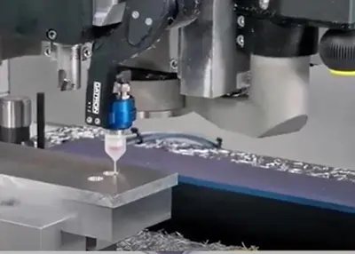 What Are The 3-Axis, 4-Axis, And 5-Axis In Cnc Machining, And What Is The Difference Between Them?June 21, 20223-axis CNC machining, 4-axis CNC machining, and 5-axis CNC machining are terms that are often heard in our industry work. Some users can't tell. For these types of CNC machining, there are still C...view
 Pop Rivets vs. Blind Rivets: A Comparison of Two Common FastenersNovember 28, 2023Fasteners are devices that are used to join or hold two or more materials or parts together. There are many types and categories of fasteners, such as screws, bolts, nuts, washers, nails, pins, etc.view
 How Much Do You Know About Stainless Steel Knowledge?October 23, 2023Steel, is a generic term for iron-carbon alloys that contain between 0.02% and 2.11% carbon. When the carbon content is greater than 2.11%, it is referred to as pure iron. The chemical composition of steel can vary greatly, and steel containing only carbon is known as carbon or plain steel.view
 EN
EN
 ru
ru 


